We offer printed circuit board layout services for all types of electronic devices: analog, digital, mixed signal, as well as different levels of complexity - from simple household or industrial devices such as led lighting, power supplies, sensors and detectors, to more complex devices including embedded systems, electronic measuring instruments, single board computers, navigation systems, communication and multimedia devices.
We also can redesign the previous layout of printed circuit board, for example to amend an existing project by upgrading the land patterns (footprints) for obsolete electronic parts or optimizing the pcb for better manufacturability and assemblability and so on. We invite you to contact us and let us know your design requirements and we will complete the project as soon as possible.
Our expertise includes the following techniques:
- Single/Double sided and Multilayer (including HDI) PCB
- Rigid, flex, rigid-flex and metal core PCB
- High speed digital design, RF PCB
- Controlled impedance routing both single ended and differential, LVDS
- Signal integrity analysis
- Optimal stack-up planning, split planes design
- Micro BGA/high pin count BGA
- Microvias, blind/buried vias, vias-in-pad
- EMC/EMI controlled design
- Thermal analysis
- DFM/DFA/DTA compliance design (according IPC)
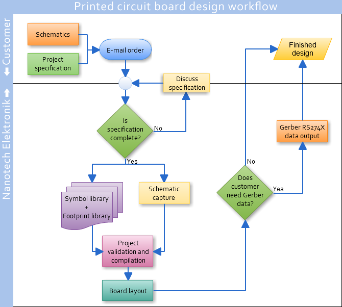
- Data output ready-to-production (Gerber RS274X)
- Cost effective design
To obtain an estimate for a PCB layout design, customers must send us their schematic drawings, which could be prepared using any CAD/CAE software, or even a scanned image. Please also include the project specifications together with a list of components and the names of the vendors and design requirements - board dimensions, number of layers, critical parts placement guides etc. Upon receiving the RFQ (request for quotation), we will send you a detailed estimate along with a time frame to complete the design.

Usually the finished PCB design project contains the following data: schematics, PCB layout, bill of material (BOM), and technical notes. According to customer requirements, we can additionally provide: 3D visualization, simulation results (signal integrity, thermal analysis and other), assembly drawings, solder paste stencil drawing, pick&place data and more.
We welcome any further questions you may have and look forward to receiving your orders for PCB design!


