Multilayer PCB Stackup Planning
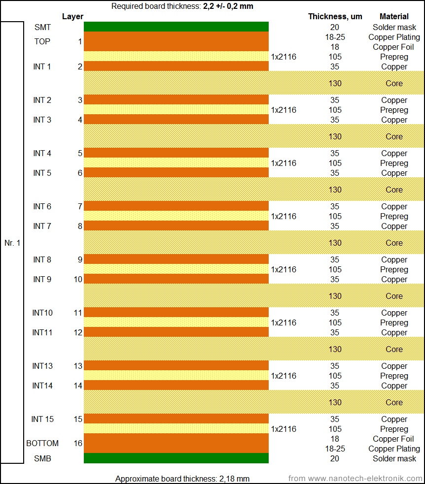
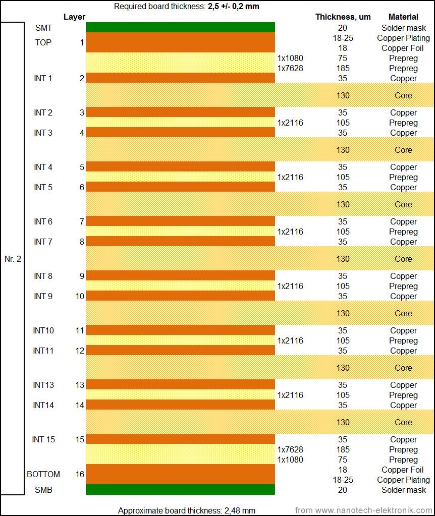
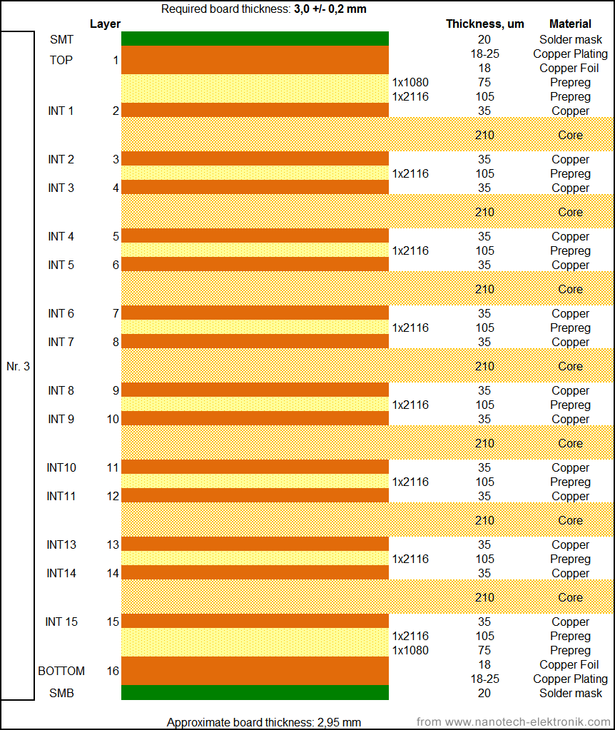
In order to properly design the multi-layer printed circuit board, one should carefully consider the design of the layer stack-up. The need for planning the layer stack-up lies, on the one hand, on the technological capabilities of the production, and on another – on the requirements to the electrical properties of the printed circuit board. The latter include the impedance control, signals integrity, noise immunity and electromagnetic compatibility. Another important thing is the optimization of the layers stack-up and interconnections from the point of view of costs. Depending on the choice of the printed circuit board structure the production costs can vary significantly.
One need to remember that the multilayer PCB consists of a combination of cores, prepregs and copper foils. For your choice we have in stock a supply of materials. For their proper selection we recommend to use the table:
| Standard copper thickness | 9 μm |
| 18 μm | |
| 35 μm | |
| 50 μm | |
| 70 μm |
| Types and thickness of prepregs | 0,075 mm (1080) |
| 0,105 mm (2116) | |
| 0,185 mm (7628) | |
| 0,216 mm (7628) |
| Standard core thickness | 0,1 mm |
| 0,13 mm | |
| 0,21 mm | |
| 0,25 mm | |
| 0,36 mm | |
| 0,51 mm | |
| 0,71 mm | |
| 1,0 mm | |
| 1,2 mm | |
| 1,6 mm | |
| 2,0 mm | |
| 2,4 (2,5) mm | |
| 3,2 mm |
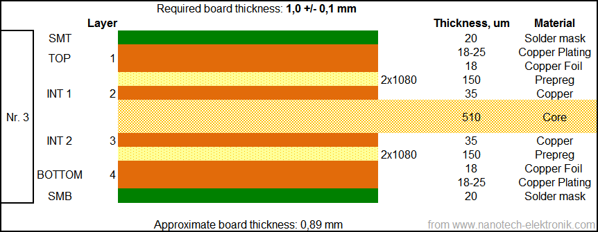
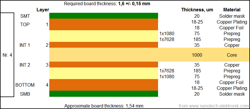
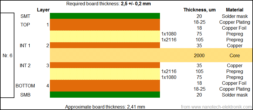
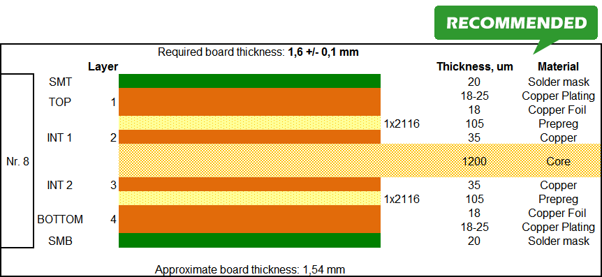
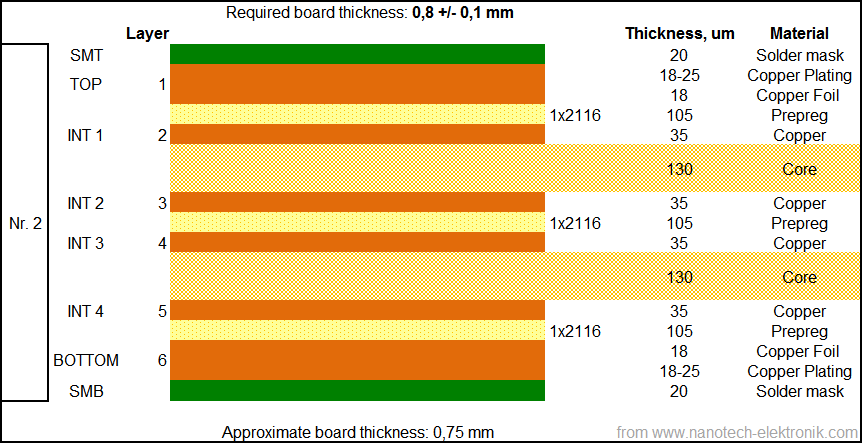
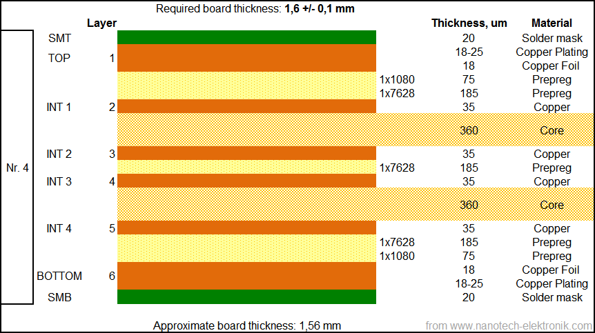
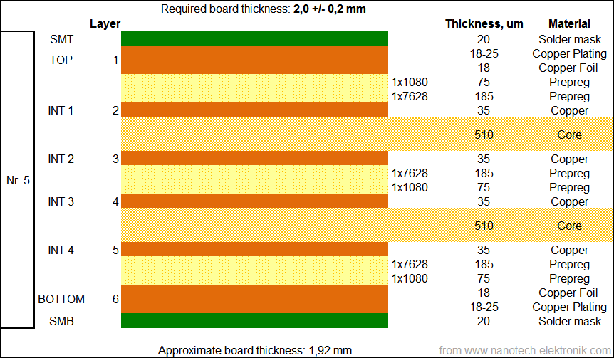
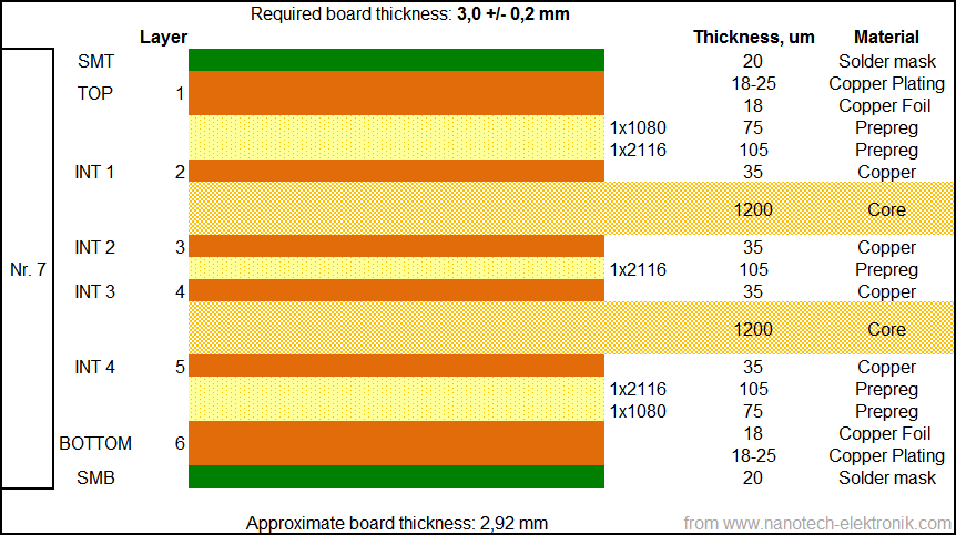
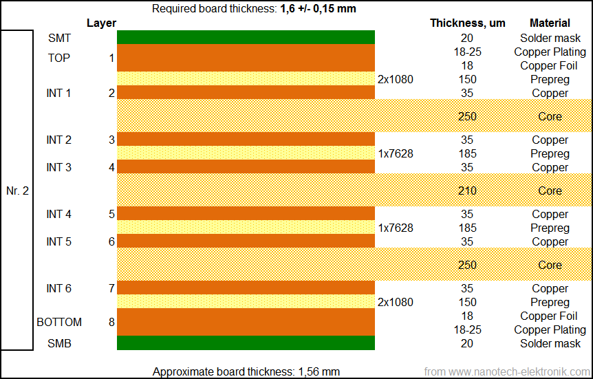
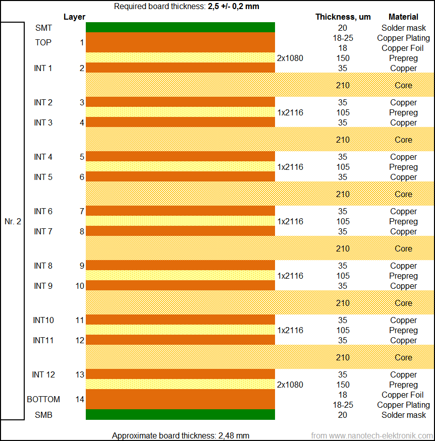
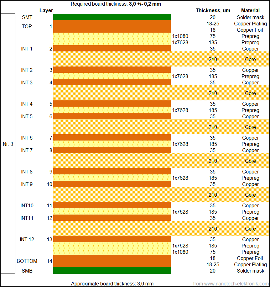
Below we put the most common designs of layers stack-up’s of printed circuit boards. The optimal ones (cheapest) we marked with the icon "Recommended".
4 layer printed circuit board




6 layer printed circuit board
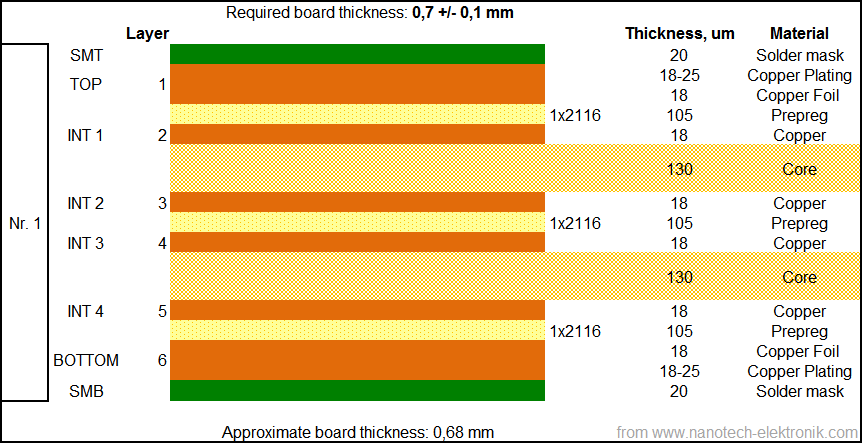


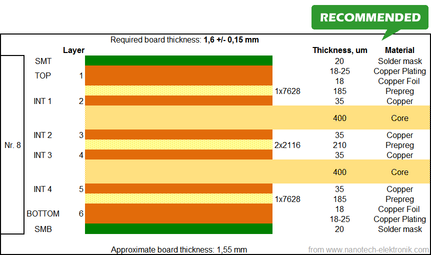
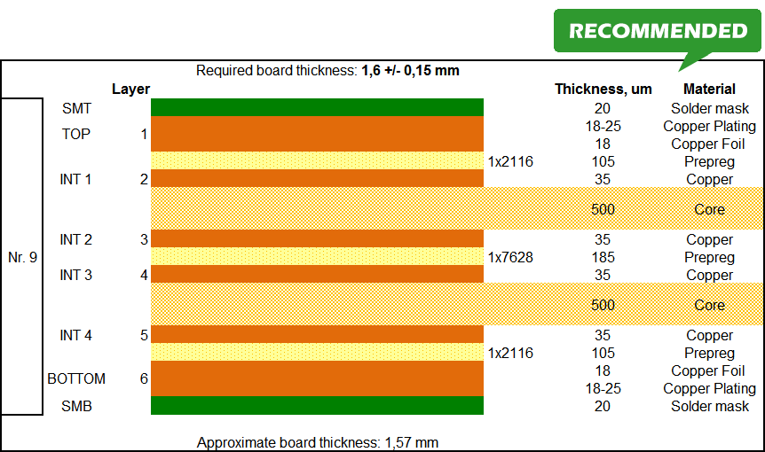
8 layer printed circuit board
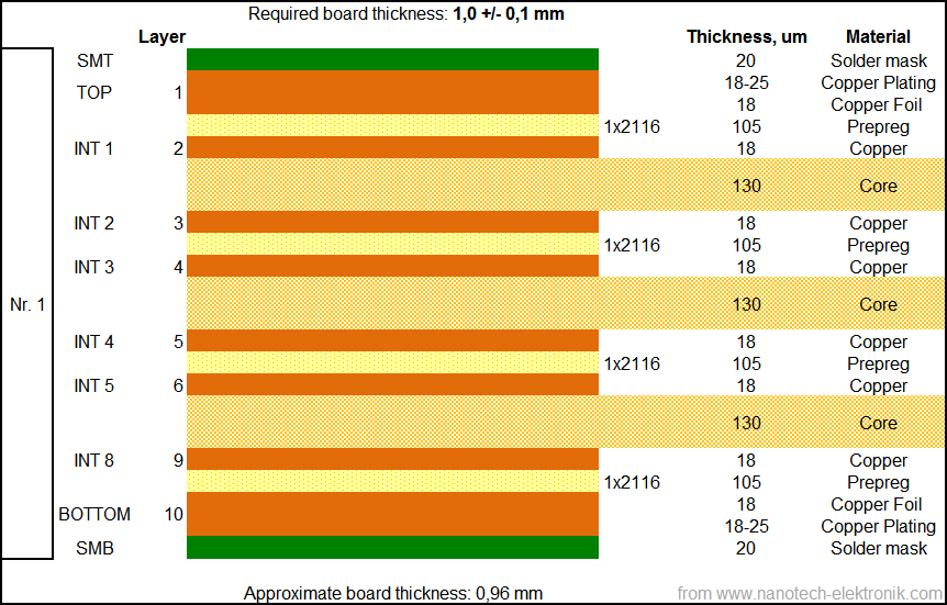


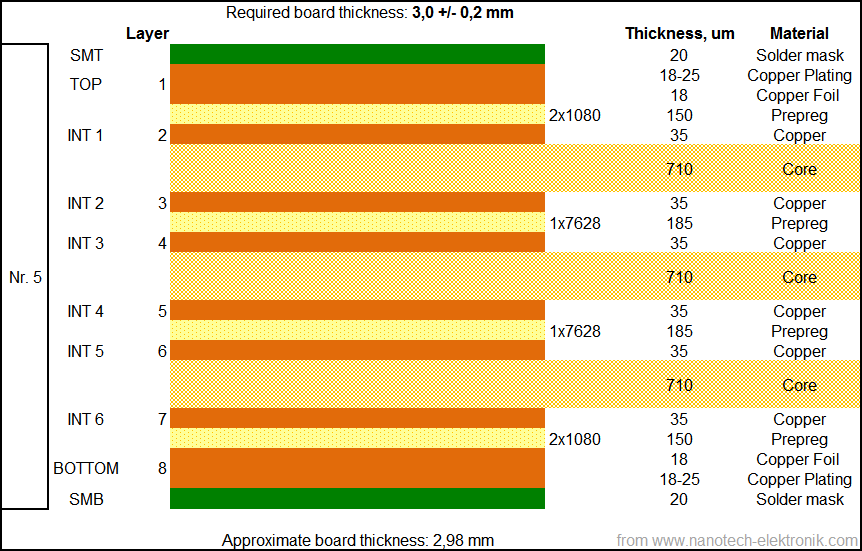
10 layer printed circuit board

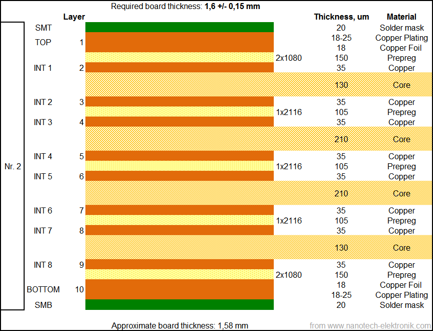
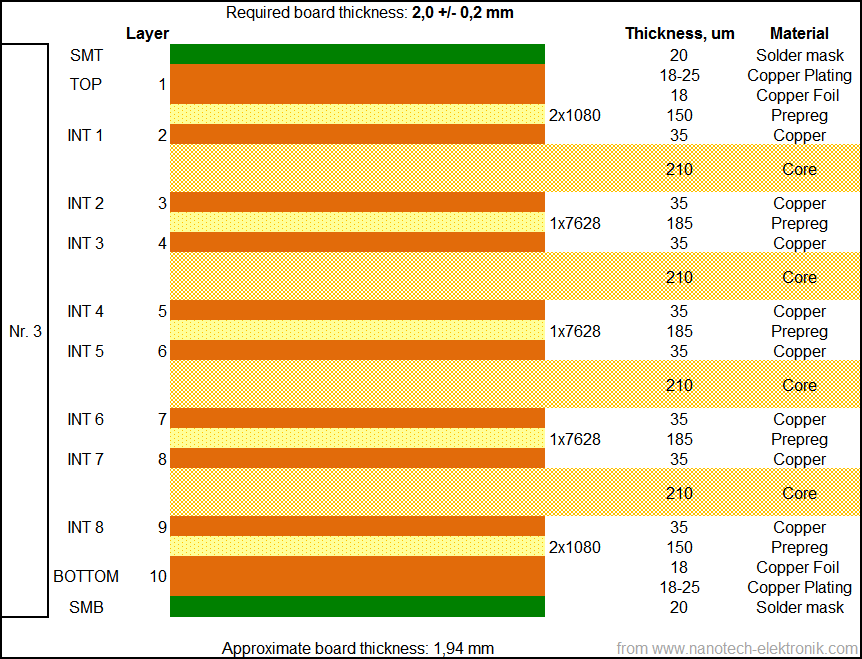
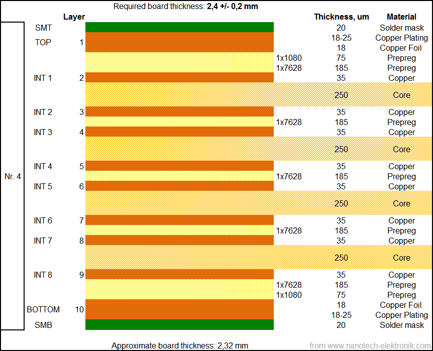
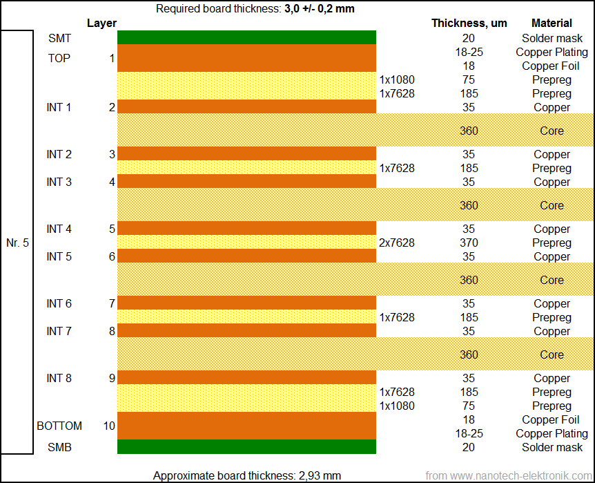
12 layer printed circuit board
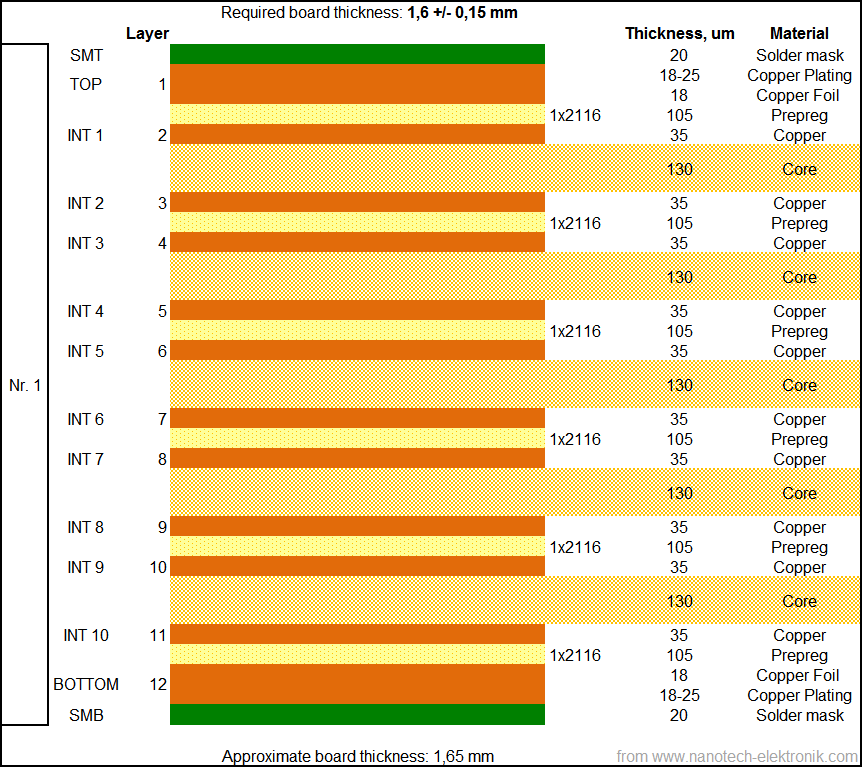
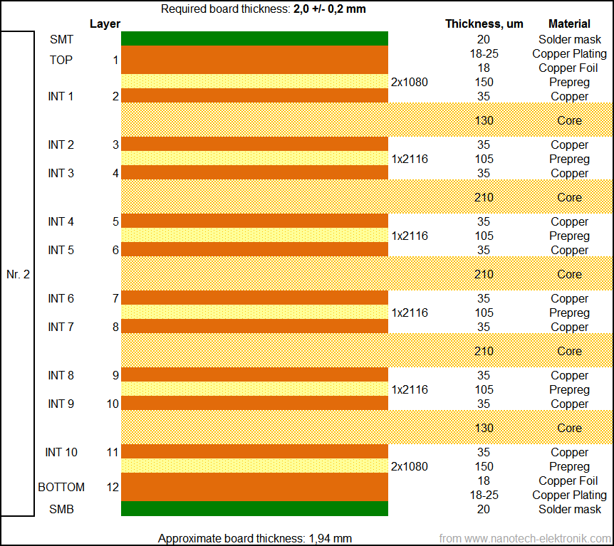
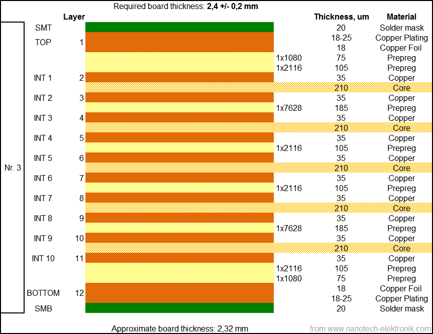
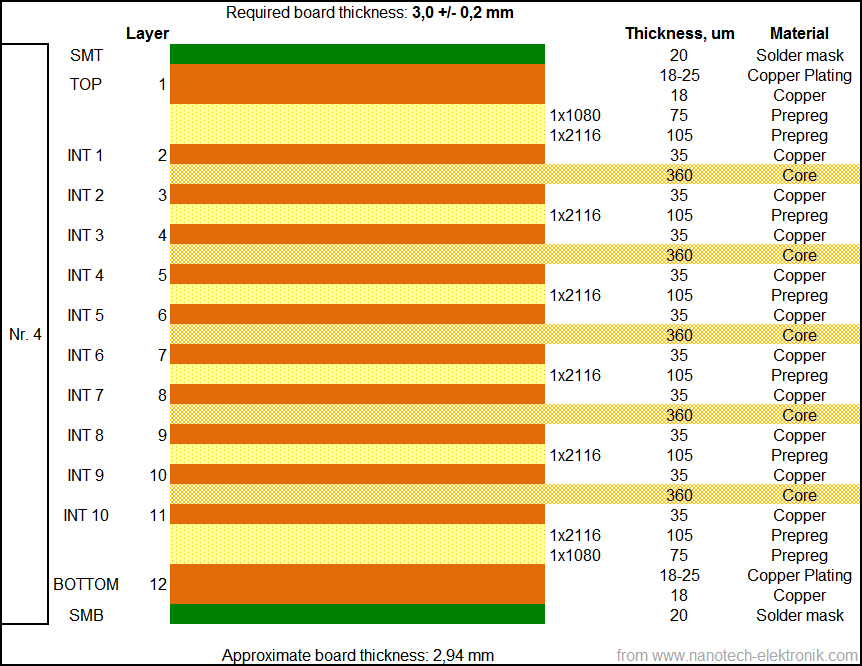
14 layer printed circuit board

16 layer printed circuit board
